Santa Clara (CA) – Last week, Intel released eight technical papers providing details about its Tera-scale project. TG Daily had an opportunity to discuss the technology with Jerry Bautista, director of technology management at Intel. Could Tera-scale become the x86 killer?
The Tera-scale project is currently has over 100 separate teams work on it. Intel is working on everything from electrical foundations all the way up to the software. Some of the research Bautista was able to share with us indicated how powerful this project is and why Intel is throwing so many resources at it.
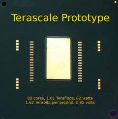
In February 2007, a prototype chip was built on 65nm process technologies. It clocked at nearly 3.16 – 5.8 GHz, had 80 separate compute cores operating internally, and it ran through six different customized benchmarks with each using traditional compute burdens. The result was a remarkable 1.01 Teraflops of parallel computing on just 62 watts of input power (1.63 Teraflops at 5.1 GHz and 175 watts, and 1.81 Teraflops at 5.7 GHz and 265 watts). While that level of computing for a single chip is impressive in and of itself, the process and mechanics of how Intel got there are at least as impressive.
Off-the-shelf logic
Intel used mostly off-the-shelf logic components for its prototype. This means that arithmetic units, memory controllers, internal routing technology, caching, and everything else, was either used exactly as it had already been developed, or with the barest minimum of customized changes. This technology re-use enabled Intel to take a research project from drawing board to prototype in less than a year. The Tera-scale project was first announced publicly in March, 2006.
Tile design
One of the most powerful features of Tera-scale is the cookie-cutter like nature of its design. We were told by Bautista that it does not really matter what compute engines are inside each core. In fact, when Intel was designing the overall system, the actual contents of the compute cores were literally of almost no importance. First and foremost was the scalable bus architecture, which allowed any one of cores to communicate directly with any of the others. Bautista called this a “one to any” communication method.
The prototype itself used 80 homogeneous cores. We were told it could have used any number, and they did not have to be homogeneous. The reason Intel chose 80 cores was because the design specs allowed for a certain number of transistors. And basically with the memory/logic tradeoff they had in mind, the company settled on the 80-core number because it provided enough memory and compute cores to prove the new idea works. It could have just as easily been 200 cores, 50 cores, or any other number because of the on-board communication system, Bautista said.
Communication
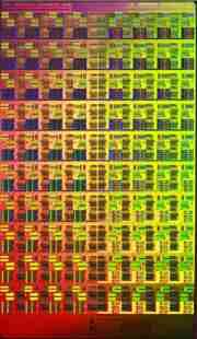
Intel uses a tier-based communications system for Tera-scale. The overall design was comprised of ten blocks of eight cores each, called nodes. Each node can communicate with any other node, and subsequently to any other core within the whole CPU. Each core communicates directly with every other core in its node, but uses the node-to-node routing system for everything external to its node.
Bautista stressed that this generic routing system is the highlight of Tera-scale. It allows anything within a node to communicate with anything else on chip.
In addition, cores do not have to be just general compute cores. They can be of any specialized design. In fact, a single node could have an array of heterogeneous cores within. And even more, each node does not have to have anything except the external communication router technology which allows it to communicate with every other node. This means that each node does not have to be comprised of compute cores. As far as the design goes, each node could be anything. DSPs, compute cores, parallel FP engines, anything.
Take special note about what this means and just how powerful it is. Intel has designed a system which encapsulates all of the components necessary for a multi-computer system, but the company has done so on a single die. There is a powerful node-to-node communication protocol which holds it all together, which makes Tera-scale CPUs able to come off the assembly line with widely varying compute abilities. As long as each node is built to spec, it can literally be dropped in, or as many of them as are necessary could be dropped in, resulting in amazingly varied compute abilities for whatever task is targeted.
Does your application needs lots and lots of parallel floating point compute abilities? Add some extra FP nodes. What about high-speed integer processing? Add some specialized RISC cores. Or maybe high-end memory bandwidth and very large caches? Then add a high-cache node to support block operations.
The cookie-cutter nature of this design allows flexibility in compute abilities that we are not used to. New processors with more FP, more integer, more fusion-like technology combining GPU + CPU compute abilities, etc. These are all possible very quickly if they are designed to Tera-scale’s protocols.
Implementation
The Tera-scale prototype was built in layers. The memory sits on the bottom of the chip. It communicates vertically with the core, which is above. Each core has a dedicated 64 MB of RAM to itself. With 80 cores, that was only 5.12 GB, but Intel was limited by the design specs and a certain number of transistors.
The communication system was implemented quickly using off-the-shelf components of what Intel already had developed. It had somewhat limited bandwidth, though even without being customized as it would be for a final product, it achieved an aggregate bandwidth of 1.2 TB/s.
The prototype also used a reduced clock signal distribution system. Whereas traditional CPUs assign about 30% of their power budget to clock distribution, according to Bautista, Tera-scale uses only about 10%, which was enabled by having fewer “repeaters” throughout.
This allowed the ones Intel had in place to communicate their signals to more distant locations with less power. The problem the company had to overcome using this solution, though, was that the clock signals arrived at their more distant destinations nearly a fully cycle out of phase. To accommodate this, Intel just did the math; Clock signals were mathematically adjusted for how far out of phase they would be at certain points. This allowed all clock signals to be properly in sync with much less power and greater flexibility.
Read on the next page: Routing, self-correction, caching and design of the Tera-scale chip
Routing
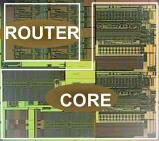
The router system is another impressive part of this design. Each core itself has an on-board router that can communicate in six directions. These are the traditional north, south, east, west paths, which allow the eight-cores to address their neighbors on any side. But there is also a logical up and down, which relate to memory and node communications.
Each core communicates directly with the cores adjacent to them. Those cores along the edge without any additional cores out there use termination logic. Likewise, each node does the same. This is where the scalability comes from. By designing a single node, which was comprised of a single core design replicated eight times, Tera-scale was able to be created with 10 blocks of these nodes.
With Tera-scale, it doesn’t really matter what’s out there in those other nodes. They just need to be able to talk to one another. And with the routing system Intel has designed, it looks like it is a piece of cake.
Bautista called the process “wormhole routing”. It allows physical pathways to be setup by an initial request sent from A to B. When the pathway is established, the sender sends n packets of data. Once received, the receiver sends back an acknowledgment signal that everything was received without error. Then, the pathway is closed. In this way, every router between A and B knows exactly how much is coming. And after it’s sent, those routers can automatically realign themselves for whatever workload comes next.
In terms of silicon real-estate, a considerable portion of each core in the prototype was dedicated to the router. However, the compute units in the prototype were very simplistic. In future designs, the compute units will be more complex and capable, we were told. As a result, their larger logic will dwarf the router.
Self-correction
If a core fails a self-test of some kind, it can signal to other cores that it’s no longer functioning. The routing system will automatically accommodate for this failing without any software intervention. This ability would allow a large core-count Tera-scale CPU to continue operating with the remaining cores, even if one or several of them have failed.
In addition, entire core workloads can be shifted around at will by the hardware. Bautista described this ability as being part of a way to control heat, utilize more cache, and other advantages. Intel realized that by shifting some of the core’s workloads to other more distant locations, then the heat and caching requirements can be spread out and the chip will be cooled and utilized more efficiently.
The routing system is capable of handling the complete migration of any physical core’s workload completely automatically. To all external software, nothing has changed. The OS still thinks that core #15 is working on the task, even though core #72 might now be doing it. This internal aliasing appears to be very powerful and is provided free of charge by the system Intel has come up with.
Big milestone
What makes the Tera-scale prototype interesting, of course, is foremost its tile design coupled to the reusability of constructed cores and nodes.
By allowing each node to communicate with other components, no matter what they might be, Intel introduces a new ability in microprocessor design – similar to what AMD has described for its upcoming Fusion processor. For example, Bautista told us that GPU logic could be created within a node. The same goes for massively parallel floating point units such as ClearSpeed’s CSX600. Even DSPs, Gigabit Ethernet, entire video solutions, the bulk of the chipset, anything. Any kind of silicon-based product that can exist today can be injected into this design, at least in theory. It is just a matter of how many resources want to be converted in this way.
Even IA-32 cores could be integrated into the Tera-scale chip. An implementation of the Exoskeleton solution that Intel has been working on for IA-32 would allow the non-IA-32 cores to be presented to external software as if they were IA-32. This virtualization of compute resources opens up another door for the future.
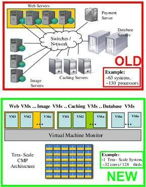
One simulation Intel ran on a Tera-scale chip of the future involved replacing a 130-processor e-commerce system with a single Tera-scale CPU. The real-world system was comprised of 63 boxes and 130 processors. Intel accomplished the same workload and throughput with 1 Tera-scale processor, which housed 32 cores and 128 threads, Bautista told us.
Caching architecture
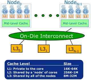
Future Tera-scale CPUs will implement a three-level caching system. The L1 cache will be tightly coupled to each compute core, and will be 16-64 KB in size. An L2 cache of 256-1024 KB will be shared by each node. And the entire CPU itself (all nodes) will share an 8-32 MB L3 cache. All of these will be on the same die as the compute cores, routers, and everything else.
Intel has also shown a new, tightly coupled high capacity L4 cache which could be oriented in such a way that it sits sandwiched between processor and the memory. Or, it could be sitting next to the processor. There are benefits and drawbacks to each design, and Intel is researching them at this time, we were told.

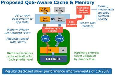
Priority routing for cache and off-chip communication requests will also be available via a type of real time QoS (Quality of Service) setting. The proposed solution indicates that implementing QoS results in a 10-20% speedup over the straight-forward “first come, first served” approach. There are things that are often known to need higher-priority access to data or communications. When properly implemented, it makes everything run faster.
Design process
Bautista indicated in a podcast that Intel came into the Tera-scale project by looking at a wide range of future software needs and then asking the question of: How do we get there? Apparently, Intel saw the software first and moved to the compute requirements from there.
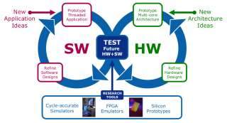
Intel said that it is using a wide array of tools for development and testing. These include cycle-accurate simulators, FPGA emulators and true silicon prototypes. The firm’s stated discovery processes for both hardware and software involves trying an idea, prototyping it, building it, testing it, modifying software for it, then revisiting the idea and beginning again. With enough passes through this cycle, Tera-scale will be flushed out.
Availability
Bautista indicated that research is moving forward fast. Still, there are many hurdles to be overcome and much design work to do for true production-ready chips. While he would not give a specific date when products would be available, he did inform us that the software they looked at in their early analysis work was 5-10 years out. It is likely they’re positioning this chip to be there when the software workloads are really needed. This could make Tera-scale available sometime in that 5-10 year timeline, possibly as early as 2012.
Conclusion
Tera-scale is a highly flexible base platform design, which has the potential to lead the way to many more possibilities. The technology can allow massively parallel operations in a MIMD model, which is “Multiple Instruction, Multiple Data”. It can do this using a traditional multi-core model or through the addition of specialized cores.
If things progress as this early research suggests, then Intel’s Tera-scale processor may finally be the processor which does two significant things. First, it will provide massive computing capacity with low power. Second, we have no doubt that there is a very real potential that this design approach may replace the x86 architecture we know today rather sooner than later.