IBM’s developed a new optical communications link that, it says, allows massive amounts of data to be transmitted with record-breaking low power consumption.
The DARPA-funded team says the technology could form the basis of exascale computers that could model the global climate, run molecular-level simulations of entire cells, design nanostructures, and more.
“We envision machines reaching the exascale mark around 2020, but a great deal of research must be done to make this possible,” says Jonathan E. Proesel of the IBM T. J. Watson Research Center.
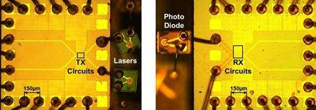
Proesel and his colleagues combined circuits in IBM’s 32-nanometer silicon-on-insulator complementary metal-oxide-semiconductor (SOI CMOS) technology with advanced vertical cavity surface emitting lasers (VCSELs) and photodetectors fabricated by Sumitomo Electric Device Innovations USA.
The result was a power-efficient optical communication link that can operate at 25 gigabits per second – but which uses just 24 milliwatts of total wall-plug power, or 1 pJ/bit.
“Compared to our previous work, we have increased the speed by 66 percent while cutting the power in half,” says Proesel. “We’re continuing the push for lower power and higher speed in optical communications. There will always be demand to move more data with less energy, and that’s what we’re working toward.”