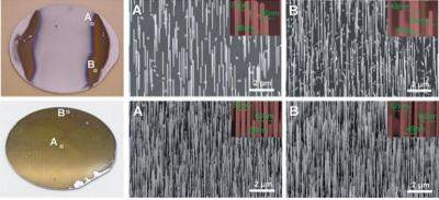
An international research team has demonstrated a novel method to epitaxially synthesize structurally and compositionally homogeneous and spatially uniform ternary InAsyP1-y nanowire on Si at wafer-scale using metal-organic chemical vapor deposition (MOCVD).
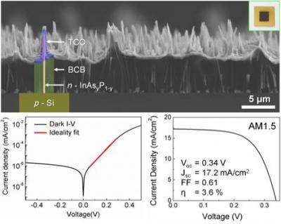
The high quality of the nanowires is reflected in the remarkably narrow PL and X-ray peak width and extremely low ideality factor in the InAsyP1-y nanowire/Si diode.
A nanowire is a nanostructure with a diameter of the order of a nanometer (10-9 meters). Alternatively, nanowires can be defined as structures that have a thickness or diameter constrained to tens of nanometers or less and an unconstrained length. Technology related to nanowires has been selected as one of the 10 Breakthrough Technologies of 2004 by MIT Technology Review.
High-aspect-ratio semiconductors have led to significant breakthroughs in conventional electrical, optical, and energy harvesting devices. Among such structures, III-V semiconductor nanowires offer unique properties arising from their high electron mobility and absorption coefficients, as well as their direct bandgaps.
A common technique for creating a nanowire is Vapor-Liquid-Solid (VLS) synthesis. This process can produce crystalline nanowires of some semiconductor materials. However, metal catalysts, usually expensive noble metals, should be used for initiating the VLS mechanism. In addition, these metal catalysts are known to significantly degrade the quality of semiconductor nanowires by creating deep levels, thus limiting practical applications of nanowires into opto-electronic devices.
In this work, however, Prof. Choi’s group developed a novel technique of growing III-V semiconductor nanowires without metal catalysts or nano-patterning. Metal-organic chemical vapor deposition (MOCVD, AIXTRON A200) was used for the growth of the InAsyP1-y. 2 inch Si (111) wafer was cleaned with buffer oxide etch for 1 minute and deionized (DI) water for 2 seconds.
Then, the wafer was immediately dipped in poly-L-lysine solution (Sigma-Aldrich inc.) for 3 minutes then rinsed in DI water for 10 seconds. The Si substrate was then loaded into the MOCVD reactor without any delay. The reactor pressure was lowered to 50 mbar with 15liter/min of hydrogen gas flow. Then the reactor was heated to growth temperatures (570 – 630 ℃), and stabilized for 10 minutes.
Kyoung Jin Choi, Associate Professor at Ulsan National Institute of Science and Technology (UNIST), Korea, and Xiuling Li, Professor at University of Illinois, U.S.A. led the research and this description of the new research was published on the web on May 7 in ACS Nano. (Title: Wafer-Scale Production of Uniform InAsyP1-y Nanowire Array on Silicon for Heterogeneous Integration).
“If we develop new technology which manages the density of nanowire and bandgap energy with further study, it is also possible to produce high-efficiency & low-cost large scale solar cells,” said Prof. Choi. “This technology will give us a chance to lead the research on the new renewable energy.”